Mass production of nanowire powders using direct reaction of the component elements
In this project, nanowire mass production process has been improved to ensure that all the raw materials supplied react and form nanowires without the associated formation of any byproducts, such as nanoparticles. For example, zinc supplied as flakes completely reacted with the phosphorus supplied via the vapor phase and lead to the formation of pure Zn3P2 nanowires. In essence, no unreacted zinc remains mixed with the Zn3P2 nanowires by the end of the experimental run. The process conditions have also been optimized to ensure that no other byproducts (e.g., Zn3P2 nanoparticles) form during the process. This byproduct-free nanowire synthesis has been reported in the Journal Materials Research Express (5, 055042, 2018). A pictorial summary of the results of this work is provided below.

Simultaneous consolidation and alignment of nanowires using equal channel angular extrusion (ECAE)
In this project, we have utilized equal channel angular extrusion (ECAE) as a tool for the simultaneous consolidation and alignment of nanowires. The idea here is to obtain bulk assemblies of aligned nanowires, without the use any flow-based technique (e.g., Langmuir-Blodgett films for nanowire alignment). To achieve the simultaneous consolidation and alignment of nanowires, a copper billet filled with silicon nanowires is extruded through two identical channels that intersect perpendicular to each other. The results indicated that consolidation of nanowires is possible even at room temperature. In certain regions, the nanowires were also found to be highly aligned. A pictorial representation of the process and the results is shown below (Materials Research Express, 2, 015013, 2015).

Non-conformal Decoration of Semiconductor Nanowires as a Novel Route for Imparting them Stabilities Against Water- and Acid-assisted Degradation
The aim of this project is to develop a strategy for imparting stabilities to water- and acid-assisted degradation to semiconductor nanowires useful in the fabrication of photovoltaics (Zn3P2) and thermoelectrics (Mg2Si). We anticipated that such a strategy is essential for the widespread deployment and use of nanowire-based energy conversion devices, as such devices will be exposed to rainwater during operation and use and rainwater is acidic in nature (pH of rainwater is ≈ 5.6). Our idea is to ensure that any strategy developed for imparting stabilities to semiconductor nanowires does not majorly impact their electrical (e.g., conductivity) and electronic (e.g., bandgap) properties. We also wanted to ensure that the strategy imparts stabilities to nanowires even at elevated temperatures as thermoelectrics devices operate at elevated temperatures. To operate within these constraints, we have developed a non-conformal BN decoration strategy that made the nanowires surfaces non-wettable by water and aqueous acidic solutions. The non-wettable nature ensured that the nanowires are resistant to water- and acid-assisted degradation. These non-conformal BN decorations also ensured that the bandgap of the nanowires, and the interfacial electrical conductivity between the nanowires in nanowire mats, are not altered. So far, we have demonstrated that nanowires of Zn3P2, ZnO and Mg2Si nanowires could be made very stable using this strategy.

Thermoelectric Properties of Bulk Nanowire Assemblies
In this project, we have evaluated the thermoelectric properties of large-scale, high dense assemblies of nanowires. We have also enhanced the thermoelectric performance of the large-scale semiconductor nanowire pellets by optimally doping them with metals. Some of the salient results achieved from this research project include the following: a p-type zT value of 0.23 in copper-doped Zn3P2 nanowire pellets (this is more than two orders of magnitude higher than that observed in undoped Zn3P2 nanowire assemblies), and an n-type zT value of 0.6 in aluminum and gallium doped ZnO nanowire pellets (the highest reported zT values for any metal oxide system). In the process of enhancing the thermoelectric properties of bulk nanowire assemblies, electrical, thermal and mechanical properties of the nanowires have been engineered through compositional and size (nanowire diameter) variations. These results indicate that inexpensive thermoelectric modules could be mass produced using materials composed of earth abundant elements (see figure below).

Simultaneous Synthesis and Assembly (via welding) of Metal Silicide Nanowires
In this project, we have developed a solid-state phase transformation strategy for the simultaneous synthesis and assembly via welding, of metal silicide nanowires. More specifically, we have tuned the nucleation and growth steps involved in the phase transformation of silicon nanowires into Mg2Si nanowires. This allowed us to phase transform pre-synthesized single-crystalline silicon nanowires into single-crystalline Mg2Si nanowires. In the second phase of this project, we have extended this solid-state phase transformation strategy and phase transformed nanoparticle decorated silicon nanowires into welded Mg2Si nanowire networks. These welded Mg2Si nanowire networks have single-crystalline Mg2Si nanowires connected together through Mg2Si bridges. The welded Mg2Si nanowire networks do not have any insulating MgO at the nanowire interfaces and therefore have highways for electron transport through the assemblies. This makes them ideal building blocks for thermoelectrics fabrication.

A schematic representing the steps involved in the synthesis and welding of single-crystalline Mg2Si nanowires for the formation of Mg2Si nanowire networks. Chemistry of Materials, 26, 2814, 2014
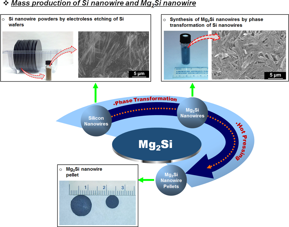
Mass production of Silicon and Metal Silicide Nanowires using a combination of electroless etching and phase transformation
In this project, we have developed a simple, but scalable, method for the mass production of compound semiconductor metal silicide nanowire powders. For accomplishing this task, we have studied the process of phase transformation in nanowires. In the first study, silicon nanowires obtained using electroless etching were phase transformed into Mg2Si nanowires by reacting them with magnesium supplied via the vapor phase. Although the process resulted in the retention of nanowire morphology after silicon was completely converted into Mg2Si, it resulted in the formation of polycrystalline Mg2Si nanowires. The diffusion of magnesium into the silicon nanowires, and its subsequent reaction led to the formation of multiple Mg2Si nuclei inside each nanowire. Further growth of these nuclei is believed to be responsible for the formation of polycrystalline Mg2Si nanowires. More recently, we have modified the process and employed solid-state reaction of magnesium foils with tapered silicon nanowire arrays for obtaining single-crystalline Mg2Si nanowires from single-crystalline Mg2Si nanowires. We believe that this process is useful for the mass production of many metal silicide nanowire thermoelectric materials.

Schematic of the three-zone tube furnace employed for the synthesis and in-situ functionalization of Zn3P2 nanowires, indicating the placement of the coiled zinc foil employed for the large-scale synthesis of Zn3P2 nanowires using phosphorus vapor transport onto zinc foils. Physical Chemistry Chemical Physics 15 (17), 6260-6267 (2013) - Reproduced by permission of the PCCP Owner Societies.
Mass production of nanowire powders using direct reaction of the component elements
In this project, we have developed a simple, but scalable, process for the mass production of compound semiconductor nanowire powders. We employ direct reaction of the component elements for the mass production of nanowire powders. For instance, we employed the direct reaction of zinc foils with phosphorus for the formation of Zn3P2 nanowires on top of the foil surfaces. Here, the foils serve as both the source and the substrates for nanowire formation. In order to enhance the surface area of foil available for the formation of nanowires, we have coiled the zinc foils as illustrated in the picture. Following the synthesis, the foil was uncoiled and brushed off to collect 100% phase-pure Zn3P2 nanowires. We have also extended this process for the synthesis of Zn4Sb3 nanowires. The synthesis procedure could also be extended for the production of in-situ functionalized compound semiconductor nanowire powders. Accomplishing this simply requires exposing the nanowires to a vapor of the requisite organic functional molecules immediately after the conclusion of the nanowire synthesis, and before they are removed from the vacuum procedure. Pictorial illustrations of the hot-walled chemical vapor deposition setup useful for the mass production of nanowires, along with those representing a small section of the results obtained, are provided below
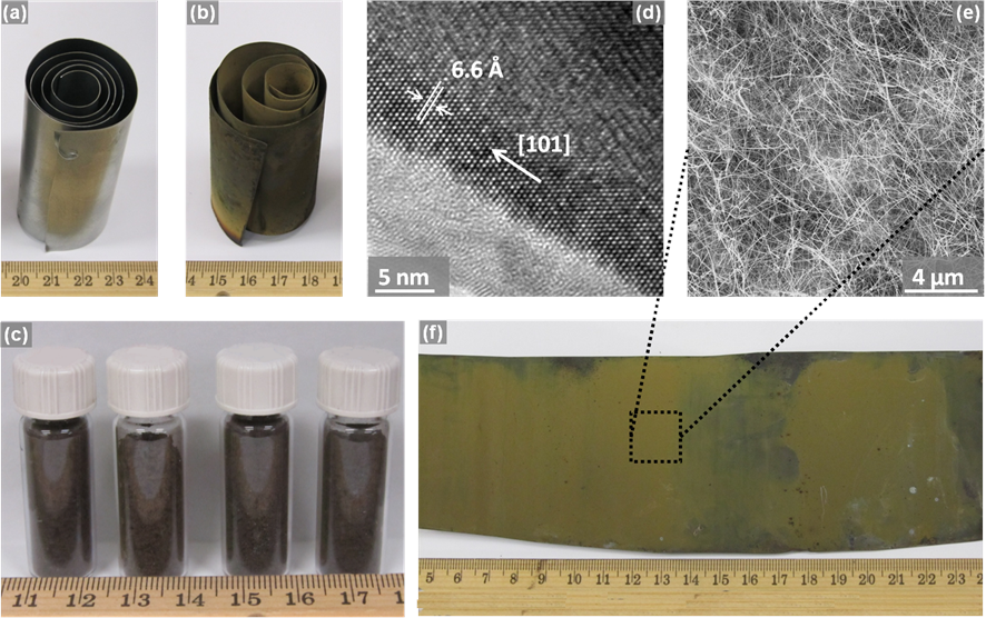
Photograph of a coiled zinc foil (a) before and (b) after the vapor transport of phosphorus. (c) Photograph of Zn3P2 nanowire powder obtained by brushing off the foils. (d) A transmission electron micrograph from a Zn3P2 nanowire indicating that the growth direction of the nanowires was not altered in the second experimental procedure and remained [101]. (e) A scanning electron micrograph of Zn3P2 nanowires obtained by the above-mentioned approach. (f) Photograph of the uncoiled zinc foil covered with Zn3P2 nanowires (green deposit) after the vapor transport of phosphorus onto its surface. Physical Chemistry Chemical Physics 15 (17), 6260-6267 (2013) - Reproduced by permission of the PCCP Owner Societies.
Bandgap Engineering of Nanowires
In this project, we have developed a post-synthesis decomposition strategy for uniformly reducing the diameters of compound semiconductor nanowires. This strategy primarily employs the ballistic transport of metal adatoms on nanowire surfaces, a phenomenon exclusive to nanoscale semiconductor materials. This ballistic diffusion of metal adatoms on top of nanowire surfaces prevents their agglomeration into droplets during decomposition and hence the breakdown of nanowires into polycrystalline matter. In fact, the ballistic diffusion of metal adatoms allows for a layer-by-layer decomposition of compound semiconductors and the formation of compound semiconductor nanowires. Using this concept, we have reduced the diameters of GaN nanowires and obtained GaN quantum wires with diameters as small as 3-4 nm. This allowed for engineering the bandgaps of GaN from 3.4 eV to 3.9 eV. Pictorial illustrations of GaN nanowires and quantum wires are provided below

Transmission electron micrographs of (a) as-obtained GaN nanowires and nanowires observed after (b) 6 minutes and (c) 10 minutes of decomposition in NH3. HR-TEM images of (d) an as-obtained nanowire and (e) a 3.2 nm GaN nanowire after decomposition indicating that the crystal structure and growth direction did not change. Reprinted with permission from Cryst. Growth Des. 11 (10), 4559-4564 (2011) - Copyright (2011) American Chemical Society.